The global semiconductor industry is advancing into the sub-2nm architectural era, marked by gate-all-around (GAA) nanosheet transistors and high-numerical-aperture Extreme Ultraviolet (High-NA EUV) lithography scanners. According to recent 2025/2026 market intelligence published by Precedence Research (https://www.precedenceresearch.com/cleanroom-technology-market) and microelectronics technical reports from Technavio (https://www.technavio.com/report/modular-cleanroom-market-analysis), cleanroom envelope standards have been fundamentally rewritten. In these multi-billion-dollar wafer fabs, physical airborne particulates are only half the battle; the invisible nemesis is Airborne Molecular Contamination (AMC)—parts-per-trillion chemical vapors that condense onto EUV mirrors, causing permanent beam distortion and catastrophic yield crashes.
| Semiconductor Cleanroom Metric | Standard Organic Foam / Wet-Built Wall | Aerospace-Grade Aluminum Honeycomb Panel |
| Airborne Molecular Contamination (AMC) | Outgasses siloxanes & phthalates (Ruins EUV) | Zero detectable VOC outgassing (Inorganic) |
| Surface Planarity & Micro-Vibration | Bows under laminar flow pressure gradients | High flexural modulus (Dampens VC-E vibration) |
| Class A Non-Combustible Certification | Combustible core requires costly sprinkler grids | 100% Non-combustible aluminum & steel composite |
| Walkable Ceiling Maintenance Capacity | Requires heavy structural catwalk steel | Integrated walkable deck (Point load ≥ 150 kg) |
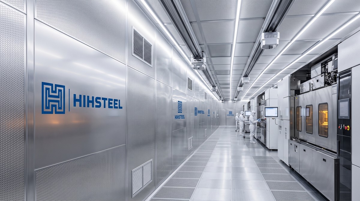
Traditional cleanroom wall panels made from organic plastic foams (such as polyurethane or polystyrene) or site-painted gypsum drywall present intolerable risks in EUV photolithography zones. Under continuous exposure to intense ultraviolet light and high room air exchange rates, organic polymers undergo micro-degradation, off-gassing trace plasticizers, siloxanes, and volatile organic compounds (VOCs). Even standard adhesives used in low-tier panels release amines and organophosphates that haze high-NA optical elements.
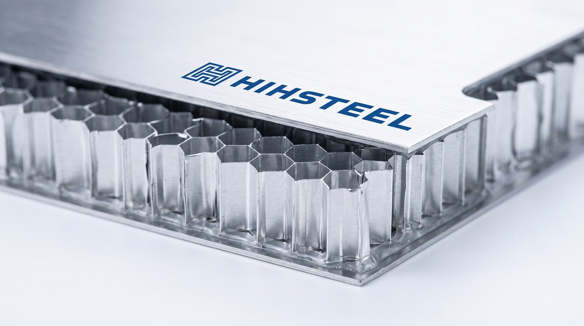
Aerospace-grade Aluminum Honeycomb Cleanroom Panels deliver complete immunity to chemical outgassing. The core consists of 100% inorganic 3003-alloy high-tensile aluminum foil formed into expanded hexagonal cells. Utilizing aerospace-grade solvent-free structural bonding films cured under high-temperature vacuum presses, the composite panel exhibits zero detectable VOC emissions, zero siloxanes, and zero plasticizer release, fully complying with SEMI F21 AMC control standards for sub-2nm wafer manufacturing.
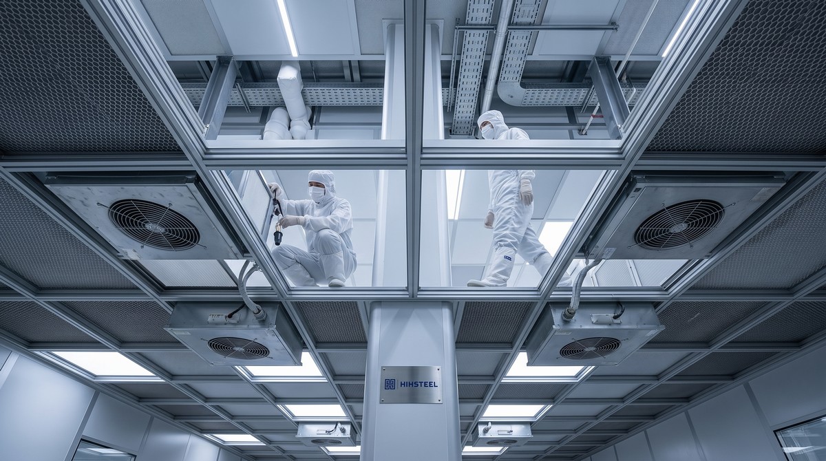
Dynamic mechanical performance is equally decisive for photolithography stability. Sub-2nm scanners are extremely sensitive to structural micro-vibrations (operating under strict VC-D and VC-E vibration criteria); laminar air currents buffeting weak partitions generate acoustic flutter that transmits into concrete sub-slabs. The cellular hexagonal geometry of aluminum honeycomb acts as an isotropic structural dampener, eliminating wall deflection over 4-meter vertical spans. Furthermore, as heavy-duty walkable ceilings spanning above thousands of Fan Filter Units (FFUs) and automated material handling system (AMHS) overhead tracks, panels easily sustain 150 kg point loads without micro-deflection, safeguarding continuous chip production.
Frequently Asked Questions (Top 5 Google Search Q&As):
Q: What is Airborne Molecular Contamination (AMC) and why is it dangerous in semiconductor fabs?
A: AMC refers to chemical pollutants in gaseous molecular vapor form (such as volatile organic compounds, siloxanes, plasticizers, phthalates, and dopants) rather than solid dust particles. In sub-2nm High-NA EUV photolithography, AMC molecules condense onto reflective multilayer mirrors and silicon wafers, causing irreversible optical beam hazing, pattern distortion, and fatal chip yield losses.
Q: Why are organic foam sandwich panels (PU/EPS) strictly prohibited in EUV lithography cleanrooms?
A: Under continuous high-intensity ultraviolet irradiation and massive laminar airflow circulation, organic polymers (like polyurethane or polystyrene) undergo micro-degradation, steadily off-gassing trace plasticizers, siloxanes, and volatile organic solvents. Even trace chemical outgassing destroys billion-dollar lithography optics, which is why foundries mandate inorganic, non-outgassing cores.
Q: What makes aluminum honeycomb panels superior for heavy-duty walkable cleanroom ceilings?
A: Aluminum honeycomb has the highest stiffness-to-weight ratio of any cleanroom core. A 50mm panel weighs only 10 to 12 kg/m² but easily supports point loads exceeding 150 to 200 kg and uniform loads over 250 kg/m² across a 1.2m–1.5m span. Maintenance technicians can walk safely across ceiling decks to service thousands of Fan Filter Units (FFUs) without micro-deflection or transmitting vibration to scanners below.
Q: How do anti-static (ESD) cleanroom panels protect nanometer semiconductor wafers from damage?
A: Semiconductor cleanroom panels feature factory-applied static-dissipative coil coatings calibrated to a surface resistivity of 10⁶ to 10⁹ Ω/sq. Integrated with copper grounding lugs connected to the facility earth ground, static electric charges bleed away in milliseconds, preventing particulate static attraction and eliminating electrostatic discharges that destroy microchips.
Q: What joint sealing system is used between aluminum honeycomb panels to maintain cleanroom positive air pressure?
A: Panels incorporate precision-milled concealed aluminum splines (‘middle-aluminum’) with double-gasket neoprene tracks and neutral-curing pharmaceutical-grade silicone sealants. When locked in place, the joint forms a completely flush, non-shedding surface tested to zero air leakage under room positive pressure differentials exceeding 50 to 80 Pa.