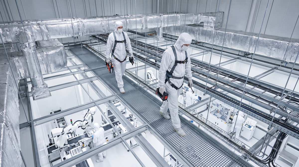
The international race for semiconductor manufacturing sovereignty has ignited the largest high-tech facility construction boom in modern history. Driven by multi-billion-dollar government incentives—including the U.S. CHIPS Act and the European Chips Act—over 18 massive semiconductor fabrication complexes are breaking ground simultaneously. As reported in global cleanroom market evaluations by Clean room Technology (https://cleanroomtechnology.com/what-is-happening-with-the-cleanroom-market-in), this unprecedented pipeline requires over 3 million square feet of high-grade (ISO Class 3 to Class 5) clean room envelopes. However, general contractors and facility engineering teams face severe bottlenecks: acute shortages of skilled trade labor and aggressive commissioning deadlines.
| Megafab Engineering Metric | Traditional Field Fabrication | Modular Pre-Engineered Clean room |
| Ceiling Walkable Load Rating | Requires separate catwalk grids | Heavy-duty structural (≥ 250 kg/m²) |
| Particulate Outgassing (AMC) | Risk of chemical plasticizer fumes | Zero-VOC baked metallic sandwich |
| Electrostatic Control (ESD) | Inconsistent site spray coatings | Factory-calibrated 10⁶ – 10⁹ Ω/sq |
| Field Installation Velocity | 150 – 200 m² per day per crew | 600 – 800 m² per day per crew |
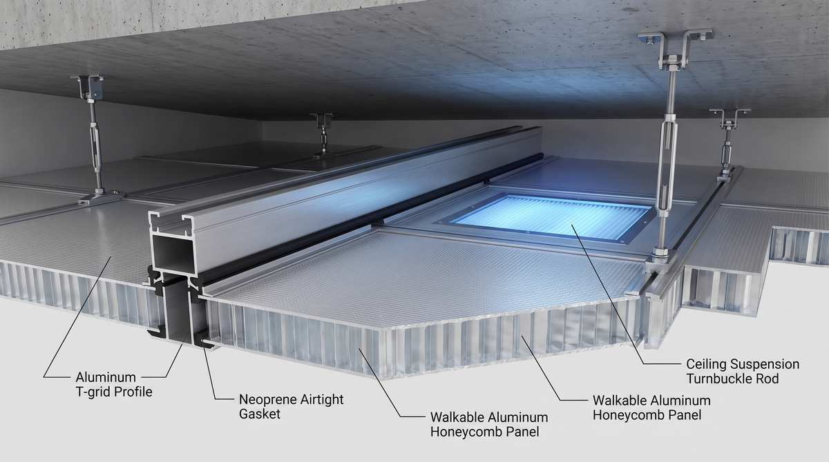
In semiconductor cleanroom construction, the ceiling plane represents the most mechanically congested boundary. Ceiling layouts must support thousands of fan filter units (FFUs), ultra-pure gas piping, exhaust ducting, and automated material handling system (AMHS) tracks. Traditional suspended ceilings require complex secondary structural catwalks for maintenance technicians, driving up steel costs and installation labor. Advanced modular cleanroom ceiling systems from the hihsteel.com Clean Room Series resolve this through structural aluminum alloy T-bar grids supporting high-density walkable aluminum honeycomb sandwich panels (thickness 50 mm to 65 mm). With point-load ratings exceeding 150 kg and distributed load capacities over 250 kg/m², maintenance engineers can safely service mechanical systems directly on the ceiling deck without interrupting live wafer production below.
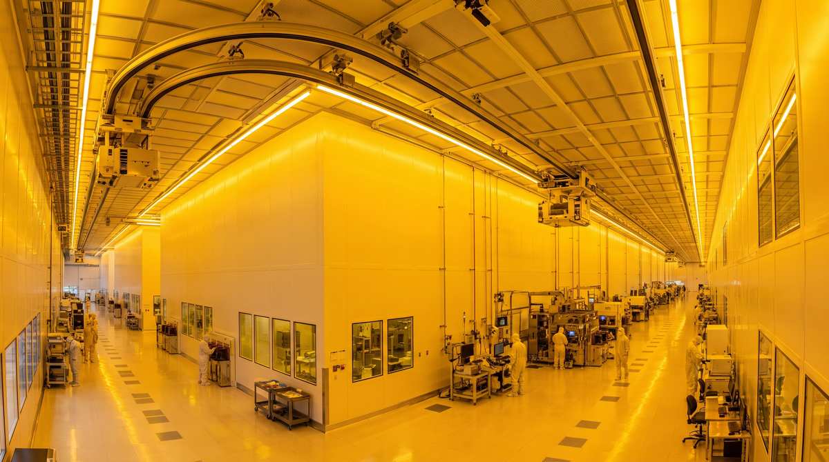
Contamination containment demands rigorous structural stability. Operating photolithography scanners require ultra-low vibration thresholds (VC-D and VC-E criteria); standard flexible partitions transmit mechanical vibrations that degrade nanometer lithographic precision. High-stiffness aluminum honeycomb wall panels feature aeronautical-grade hexagonal cellular cores permanently bonded to double-sided galvanized steel or aluminum alloy facings. The composite structure provides exceptional flexural rigidity across multi-meter vertical spans, dampening turbulent air pulses generated by laminar recirculation airflows.
Furthermore, electrostatic discharge (ESD) mitigation is factory-integrated. Premium semiconductor clean room wall panels feature static-dissipative coil coatings calibrated to a surface resistivity of 10⁶ to 10⁹ Ω/sq, tied into factory-welded earthing lugs that ground static charges before microchip-damaging voltages accumulate. By sourcing prefabricated, modular cleanroom envelopes directly from high-capacity manufacturing plants, fab EPCs achieve standardized dimensional accuracy (±0.5 mm), integrated utility raceways, and container-optimized export delivery, slashing critical-path construction schedules by several months.